The OP07 has very low input offset voltage (75 μV maximum for OP07E) that is obtained by trimming at the wafer stage. These low offset voltages generally eliminate any need for external nulling. The OP07 also features low input bias current (±4 nA for the OP07E) and high open-loop gain (200 V/mV for the OP07E). The low offset and high open-loop gain make the OP07 particularly useful for high gain instrumentation applications.
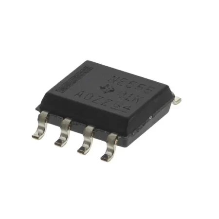
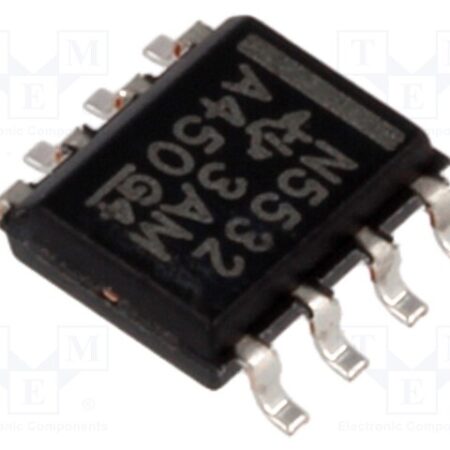
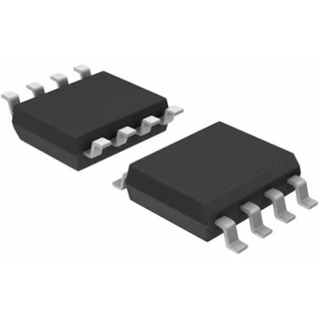
The wide input voltage range of ±13 V minimum combined with a high CMRR of 106 dB (OP07E) and high input impedance provide high accuracy in the non inverting circuit configuration. Excellent linearity and gain accuracy can be maintained even at high closed-loop gains. Stability of offsets and gain with time or variations in temperature is excellent. The accuracy and stability of the OP07, even at high gain, combined with the freedom from external nulling have made the OP07 an industry standard for instrumentation applications. The OP07 is available in two standard performance grades. The OP07E is specified for operation over the 0°C to 70°C range, and the OP07C is specified over the −40°C to +85°C temperature range. The OP07 is available in epoxy 8-lead PDIP and 8-lead narrow SOIC packages. For CERDIP and TO-99 packages and standard microcircuit drawing (SMD) versions, see the OP77.
Downloads
Datasheet






Reviews
There are no reviews yet.